In this article we will discuss how can you make PCBs using Eagle Layout Editor 5.6 Freeware (PCB design).
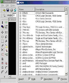
First of all Open Eagle, under Projects right click and then left click to New Project. Give a name to the new Project, for example ‘example’ and then click Enter. Right click the example, you created, and select New and then board.
 icon from tool panel in left.
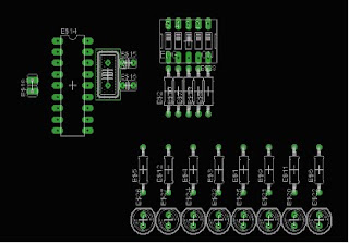
After arranging the components we get the figure like this:

You can also assign the name to the component by selecting ‘name’  icon and then chose the component which is to be named.
 icon and then chose the component which is to be named.
After tracing select the ‘polygon’  icon and draw a polygon (across the whole circuit), after doing this click on ‘Ratsnest’
  and you will get this:
 icon and draw a polygon (across the whole circuit), after doing this click on ‘Ratsnest’
  and you will get this:
 Now give the name to the polygon (for example Vcc,Vss etc) according to your signals, In my case I assign ‘GND’. Remember; also assign the same name to your signal (wire), so that the polygon and signal merge together.
 icon and then on polygon to change the polygon settings.
After applying changing in ‘spacing’ and ‘isolation’ of the polygon select the ‘Display‘  button from the tools bar and "Del" the all selections except the selected ones:
 button from the tools bar and "Del" the all selections except the selected ones:
Then click File –> Export and select ‘Image’.

This image will show up:
Change the resolution to 600 and check the monochrome box.
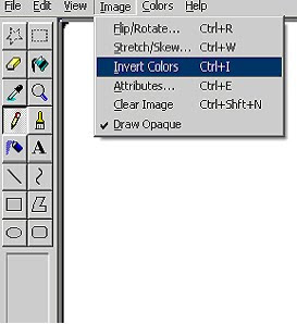
Click browse button, give name and save the image as bmp format. Open the image in mspaint select the ‘image’ option and click on ‘invert colors’.

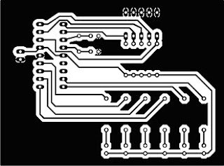
The result is like this:

You can also mirror the image by using the same ‘image’ option. Just click on ’flip/rotate’ option and select ‘flip horizontal’. Now your PCB is ready for printing.


No comments:
Post a Comment