Friday, September 3, 2010

PIC16F887/877 programming in C Tutorial 2 (S.S Display Interfacing)

Interfacing Seven Segment (c.c) Display

In this tutorial i will show you how to interface S.S display with PIC16F887/877. For this we required 74hc573 latches, 74hc238 decoder, and 74ls48 bcd2dec converter.

Latches are used to enable/disable the S.S, 74hc234 a 3x8 decoder selects the appropriate latch to be enable/disable. 74ls48 just converts the bcd input to respective decimal output to operate S.S properly. 

Now lets write a small program that display the digital manual input at S.S, enter by the user; by using 8-way dip switch.

Code:   
void main() {

     int x,y,i,j;
     trisc=0;
     portc=0;
     trisd=255;      //all bits for input

 ///////////////// comment 4 pic16f877/////////
     ansel=0;
     anselh=0;
    
     c1on_bit=0;
     c2on_bit=0;
////////////////////////////////////////////

     while(1){
       j=0;
       i=3;
       x=portd;

       while(i>0){
          y=x%10;
          y=y|j;
          delay_ms(100);
          portc=y;
          x=x/10;
          i--;
          j=j+16;

     }

  }
}

Now come towards the code; portc is utilized for o/p, and manual i/p is applied at portd, here. As the ports are 8-bit so, maximum i/p would be 255(0-255); we have to display them on three S.S, for this we have to separate the digits of i/p. Modulus '%'  do this job; let say the i/p is 255, then first we have to display 5 then 5 and then 2; to do this we use x%10. Where x is an integer that has the manual i/p. Where modulus operator returns the remainder of integer division, so after this we have 5 stored in y (as 255%10 = 5, remainder is 5).

After getting the digit, it should be display on 3rd S.S; so to select this latch just or '|' y with proper integer, which in this case is 0 (as my 3rd S.S as attached to 0 o/p of latch, 2nd is to 1st and so on). So, after doing this we have 5 in 8-bit and latch 0 is selected. Now display it by assigning it to port.

To display 2nd digit first reduce the i/p by dividing it with 10; 255/10 gives 25, as we are storing this value in an integer; so x is equal to 25, now. J is incremented by 16 because we have to select the first latch (see the diagram for more detail).


In the same fashion, to display the first digit; select proper latch, divide and take modulus and display it, that is it. Here i is used to run this process for three times (means to display all the i/p digit on three S.S).


Schematic:   
For reset circuitry  please refer to first tutorial.
connection diagram

Thursday, September 2, 2010

PIC16F887/877 programming in C Tutorial 1 (Getting Started)

PIC16F887 and PIC16F877 are the members of PIC16F88X and PIC16F87X families respectively. PIC16F887 is the new version launched by microchip to take place of PIC16F877.For detail information please refer to their datasheets.

In this tutorial i will show you how to program PIC16F887/877 in C.
So first of all download mikroc pro for pic compiler also download its user manual. After this create a new project choose P16F887 or 877 whatever you have, and 4MHz crystal etc. If you dont know how to create a new project refer to its manual or download document 'how to create first project' from its site.

Note that i will use PIC16F887 and 4MHz external crystal (although PIC16F887 also have internal crystal) you can use 8MHz and what so ever. For 4MHz oscillator setting should be XT where as for 8MHz or above it should be HS (see fig below).

Lets start with a simple program 'LED Chaser', before we start this lets check out the PIC16F887 pin out.
pinout of pic16f887
As you can see there are five multiplex i/o ports, in PIC16F887, from portA to portE. For our first program we need only one port let say portD and 5v at pins 11 & 32, ground pins 12 & 31, 4MHz xtal at pins 13 & 14. Dont be panic to see more than one name of pins, i will tell you the pin functions when we use them.

After creating the project just write the below code in mikroc ide and build it(CTRL + F9), if you want to change the project setting, fuse bits, clock etc,  goto>>project>>edit project.

Code:
void main() {
        int x[]={1,2,4,8,16,32,64,128,256};  // int array
        int i;
        portc=0;      //to clear port
        trisc=0;        //as output

///////////////////// comment this block if you are using pic16f877a/////////
        ANSEL  = 0;                        // Configure AN pins as digital I/O
        ANSELH = 0;
       
        C1ON_bit = 0;                      // Disable comparators
        C2ON_bit = 0;
 ////////////////////////////////////////////////////////////////////

 while(1){
  
      for(i=0; i<=8; i++){
         portc=x[i];
         delay_ms(100);
      }          //for bracket

         }            //while bracket 

}                //main bracket

Now come towards code; firt select the port you want to use, i this case it is portc. Then clear the port by assigning it 0. Trisx, the SFR  is used to set the port as input or output, where x can be a,b,c,d, and e; the port which you are using. Trisc=0 means the portc is selected for output. For input change it to Trisc=255; means all pins of portc as ready for input. If you want take i/p at single pin instead of whole then use trisxy_bit=1, where y could be from 0 to 7; the pin you at want to take i/p and y is the respective port.

There are two comparators in 887, to disable them assign 0 to c1 and c2 bits. Also to use pins as digital i/o assign 0 to ansel and anselh; dont be panic when we do ADC i will tell you about this. Note that for 877a these two thing is not required.

Now for loop; as for led chaser we want to on led at power of 2 sequence that is 1,2,4 till 256 as port is 8-bit so 2^8=256; that is why have save these values in a array.
To get visual we have to add some delay, to do this just write delay_ms(100); for 100 ms delay. You can increase it if you want.

As we want to see our o/p continuously not only for a single time, we use while loop; while(1) means this loop will run forever.

project setting
Schematic: 
Give the hex file path, of this project, to isis and simulate it. Dont forget to attach reset circuitry.

Reset Circuit:

Wednesday, August 25, 2010

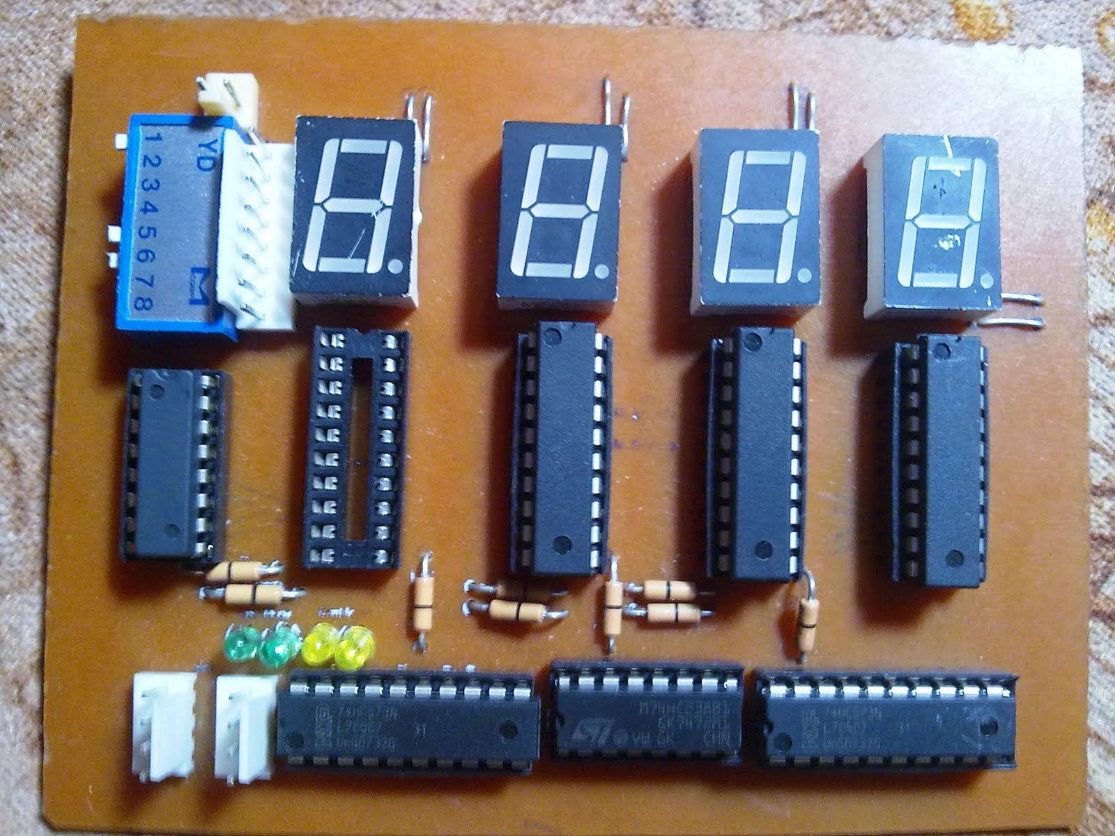
S.S Display & Manual i/p board

i used ss display and manual i/p board to interface it with 8051 Generic board, of course you can interface it with any other microcontroller. 
ICs required for this board are 74hc573 latch, 74hc238 decoder and 74ls48 BCD2dec converter . For their proper working operation refer to their datasheets.

74hc573 is used to store data so that the previous content on SS is not vanish when we disable LE pin. T0 select the proper latch 74hc238, 3x8 decoder is used. And to convert BCD into decimal, 74ls48 converter is used. Note that latches U1 to U4 are connected with C.C SS, so the output of 74ls48 will only go to these latches. Whereas latches U6 and U8 are connected to DP oF SS and LEDs respectfully. You can emit these latches i used them to distinguish between various mode i.e, digital clock, stop watch, counter and manual input etc.

For manual input DSW1 is used and J2 is the 8-way connector i used to connect it with 8051 Generic board, same for J1 connector. J3 and three switches are used to select the operating mode of this board, you can also emit these.

Note that during programming you have to be aware the J1 connections because this connector is controlling the whole board.


Schematic:


Final Assembly:
oppssss! i lost one ic


Components Required:
U1-U4,U6,U8,              74hc753
U5,                                 74ls48
U7,                                 74hc238
D1-D4,                           LEDs
D5-D8,                           SS C.C
DSW1,                            8-way dip wsitch
J1,                                  4-way jumper
J2-J3,                            8-way connector
Three button or 4-way dip switch
Zero ohm resistors 9 pics
2-way connector for power

Monday, August 23, 2010

8051 Development Board (Generic Board)

8051 Generic Board is my fist project board in 8051 microcontroller course. This board is design for atmel 89c51 ic, please refer to its datasheet for more information.

Now come towards board description:
There are four i/o ports in 89c51, this board is design in such a manner that all ports are byte addressable whare as port3 can also be access bit wise in other world port 3 is also bit addressable. This can be done by proper selecting the jumper j2 and j5 and etc.Note that there are 8 jumpers at port 3 and also 8 jumpers at the u4 & u5 o/p pins are required, whereas in schematic only four are shown.

74ls245 latches are used to decide the direction of data. Switch SW1 is used to select the direction. If SW1 is towards vcc than the data direction is from 89c51 to latch o/p pins. And if SW1 is towards gnd than the direction is from latch to 89c51. For more info please refer to its datasheet.

LED bargraph are used to indicate the status of 89c51 port pins; that is data in or out.
Connectors J1, J4 and etc are used so that we can interface this board with other boards.
Note that only port 0 and port 3 connections are shown in schematic; port 1 and port 2 connection are the same as of port 0, but in that case RP1 is not required. As port 0 needs to be pull up so, resistor pack, RP1, is only required for this port.


Schematic:


Final Assembly:


Component Layout:
 

Components Required (according to layout):
R1,                10kΩ  Resistor
R2,                100Ω  Resistor
IC1,               89c51
IC2-IC6,      74ls245
Xtal,              11.0592Mhz
C1,C2,           33pF Ceramic Capacitor
C3,                16uF/25v Electrolyte Capacitor
PB,                Push Button
Pwr,              2-way connector
J1-J11,         3-way jumper
J12-J15,       8-way connector
RB1,              10K ohm resistor bank 9 pins
PB2-PB5,     330 ohm resistor bank 9 pins
LED bargraph 4 pics
Zero ohm resistor 2 pics

Sunday, August 22, 2010

Automatic Water Level Sensor & Pump Driver

The circuit is based on a 555 IC (Bipolar or CMOS) for sensing the minimum and maximum water levels and turns a MOSFET on/off which directly controls a 12V DC pump motor. Or, it can power a relay coil to switch high currents/voltages, DC or AC.

‘Trigger’ and ‘Threshold’ pins (2 & 6) are used to detect the maximum and minimum levels, respectively. The two voltage comparator op-amps inside the 555 control the output, turning it on/off. Looking at the circuit diagram you will notice that the ‘Trigger’ pin (2) is marked ‘HIGH probe’, despite being triggered (output goes HIGH) when the voltage drops below 1/3 of the supply voltage and, the ‘Threshold’ pin (6) is marked ‘LOW probe’ while it is ‘reset’ (output goes LOW) when the voltage rises above 2/3 of the supply voltage.
The circuit works as follows:

Three (3) probes are immersed in the vessel. (usually from the top)
One is the ‘GROUND’ probe, going to the level a little lower than the minimum desired level. This is the ‘common’ (or ‘reference’) probe. The LOW and HIGH probes are set at the desired levels.

Now suppose the vessel is EMPTY.
Resistors R2 and R1 (1M) tie the ‘Trigger’ and ‘Threshold’ pins (2 & 6) to the positive (+) rail (supply). In other words, both pins are HIGH. Remember (from above), to make the output of IC1 go HIGH, the trigger pin (2) needs to drop below 1/3 of the supply voltage. (4V with a 12V supply)

Since the trigger pin is still HIGH, the output remains LOW. We need to fill the vessel when IC1’s output is LOW. TR1 is OFF. The GATE of the MOSFET switch (TR2) is connected to the supply rail (+12V) with R4 (10k). TR2 is thus turned on and the pump motor is running.
TR1 (BC547) is connected between the IC1s output (pin 3) and the TR2’s GATE. Its purpose is phase reversal. It means that when IC1’s output is HIGH, TR1 conducts and pulls its collector/TR2’s GATE junction LOW, so TR2 is OFF. Since the pump (or relay coil) is connected between the positive rail (+12V) and TR2’s DRAIN, the pump/relay coil is NOT energized.

Now, back to the condition when the IC1’s output is low, TR2’s GATE is HIGH (+12V) and conducting. The pump is operating and water is being filled. As the water level rises, a water ‘bridge’ is formed between the GROUND (common) probe and the ‘LOW probe’ (Threshold, pin 6) This ‘bridge’ constitutes a low resistance, relative to the high resistance of R2 (1M), bringing the voltage at this pin to a low level (at least below 1/3 supply but actual voltage depend on the conductivity of the water). However, this is IGNORED by IC1 since its output is already LOW (in the ‘reset’ mode).

When the water level reaches the ‘HIGH probe’, a water ‘bridge’ is formed between it and the GROUND probe. Just as with the LOW probe, this ‘bridge’ constitutes a low resistance, relative to the high value of R1 (1M), bringing the trigger voltage to below the required level (1/3 supply voltage) and IC1 triggers, its output going HIGH. Now Tr1 is turned on, the bias voltage/current of TR2 is removed and the pump STOPS. The filling cycle is completed.

As the water level falls, the ‘shorting’ water ‘bridge’ between the GROUND probe and HIGH probe (‘Trigger’, pin 2) is removed and the voltage rises above the 1/3 supply level (+4V).
This is IGNORED by IC1. [This pin needs to drop below 1/3 supply (4V) to trigger IC1. However, as long as the voltage on this pin remains below the trigger level (1/3 of supply), IC1 stays ‘triggered’, its output stays HIGH.] TR1 is conducting and so there is no bias supply to TR2’s GATE and the pump is OFF. Once the water level drops below the LOW probe (‘Threshold’, pin 6), the ‘shorting’ water ‘bridge’ disappears and the voltage rises to 2/3 supply voltage (8V), IC1 ‘resets’. (its output goes LOW)  TR1 is now OFF, having no bias current. Its collector voltage rises to the supply rail and TR2’s GATE is now biased so it is turned on and the pump is operating. This is a new filling cycle.

The circuit will repeat these actions indefinitely, as long as power is applied.

Schematic:
 
Final Assembly:

Final assembly consist of relay driver and TL power supply  


Components Required:
R1,R2,       1MΩ  Resistor
R3,R4,       10kΩ  Resistor
IC1,            555 Timer
D1,              1N4007
C1,C2,         1.uF Ceramic Capacitor
C3,              100nF Ceramic Capacitor
C4,              100uF/50v Electrolyte Capacitor
TR1,            BC547
TR2,            MTP3055